With the rapid development of information technology and the increasing demand for network, the demand for high-speed and high-bandwidth data transmission equipment is becoming increasingly urgent. As a high-speed optical module, 800G is becoming the "new darling" of data centers. In this issue, we will take a look at the technical principle of 800G OSFP 2xSR4 optical module products and its application prospects.


I.800G OSFP 2xSR4 Optical module Overview


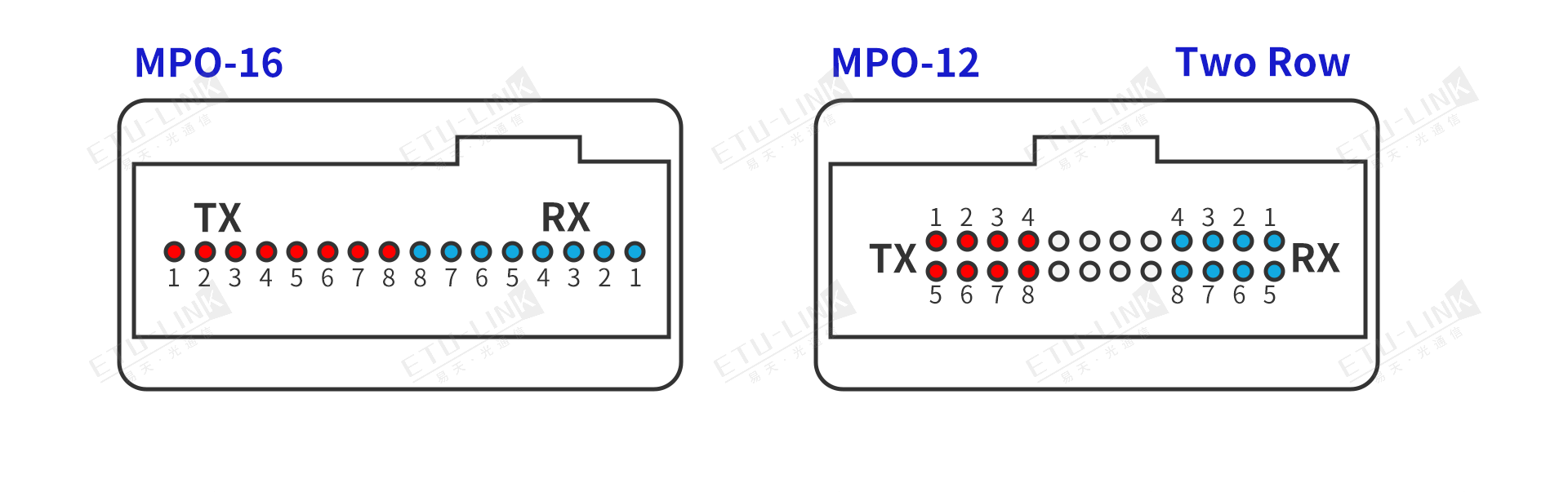
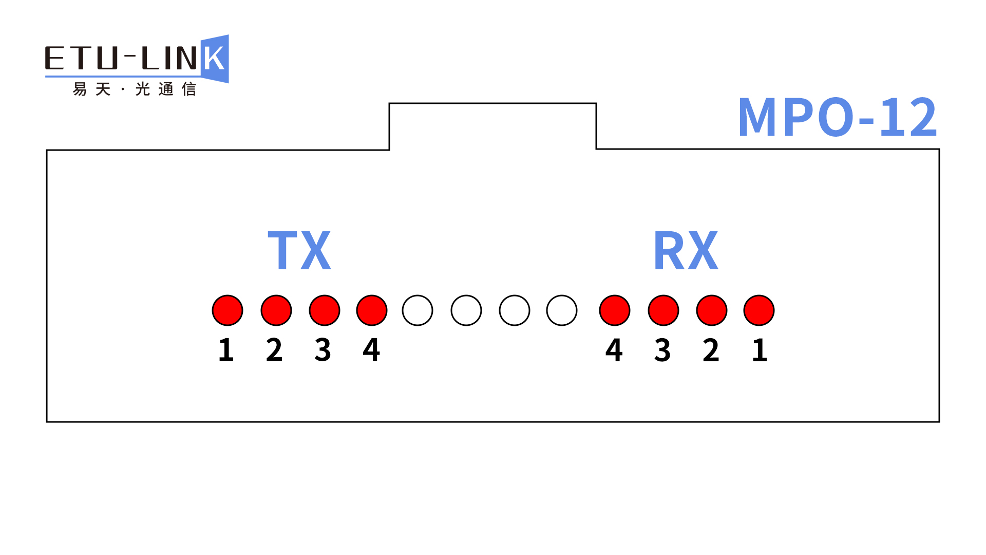
The ETU-LINK 800G OSFP 2xSR4 optical module is a fiber optic transceiver module designed for 100m optical communication applications and is designed for data center 800G SR8 Ethernet links. The module converts 8 channels of 100Gb/s(PAM4) electrical input data into 8 parallel optical signals of 100Gb/s each for a total data rate of 800Gb/s. At the receiving end, the module converts 8 channels of parallel optical signals (100Gb/s each, with a total data rate of 800Gb/s) into 8 channels of 100Gb/s(PAM4) electrical output data.

The fiber optical patch cord with dual MPO-12 connectors can be plugged into the 800G OSFP SR8 module socket, enabling 800G data interconnection up to 100m.

II. Application prospect of 800G OSFP 2xSR4 optical module


With the booming development of cloud computing, big data, artificial intelligence and other fields, the demand for high-performance network equipment continues to increase. As the representative of current technology level, 800G OSFP 2xSR4 optical module has broad application prospects.


Data centers and cloud networks: As the core of information processing and storage, data centers have extremely high requirements for high-speed, high-bandwidth network connections. The high-density design and high-speed transmission rate of the 800G OSFP 2xSR4 optical module make it an ideal choice for data center network upgrades to meet the needs of large-scale data transmission.


5G communication network: With the commercial advancement of 5G technology, the demand for optical communication technology is also increasing. The 800G OSFP 2xSR4 optical transceiver module has the advantages in transmission rate and stability, and can be used as an optical fiber transmission channel to achieve high-speed data transmission between different nodes, making it an important part of the 5G communication network to support high-speed and large-capacity data transmission.


Artificial intelligence supercomputing: The development of big data, AI technology, and intelligent supercomputing technology requires the support and matching of high-speed optical modules, so the demand for 800G optical modules will gradually increase.


This article ends here, 800G OSFP 2xSR4 optical module as a low power consumption, high reliability, economical and energy-saving pluggable optical transceiver module, its emergence for the development of modern communication technology provides a huge support power.


About ETU-LINK


ETU-LINK has been a leading manufacturer of optical modules, Dacs and AOC for nearly a decade. We are proud of not only the honor of being a high-tech enterprise, but also the rich experience we have accumulated in the field of optical modules. Whether in technological innovation or product quality, we always adhere to the pursuit of excellence, to provide customers with high-quality optical communication solutions. If you want to know more about ETU-LINK DAC products, you can send us a private message or leave a message, we will get back to you as soon as possible after receiving relevant inquiries!

With the rapid development of data centers, enterprises, vendors and users of higher, faster network demand is growing, ETU-LINK launched the 400G QSFP-DD DR4 optical module solution can better help users to solve a series of problems, the following follow the small easy to take a look at the product has what aspects of the characteristics and advantages of it!


I.400G QSFP-DD DR4 Optical Module Product Analysis


400G DR4 QSFP-DD optical module is designed to meet the needs of data center interconnections in the 400G Ethernet module, using the QSFP-DD packaging standards and PAM4 modulation technology to support up to 400Gbps data transmission rate.


The module uses 4 channels to transmit data, is IEEE802.3bs compliant, QSFP-DD CMIS Rev 4.0 compliant, and RoHS compliant, with a maximum power consumption of 12W, and it can achieve up to 500m transmission distance over Single Mode Fiber (SMF) via MPO-12 connector. Compared with other 400G optical modules, 400G QSFP-DD DR4 optical modules have lower power consumption and better heat dissipation.

II.ETU-LINK 400G QSFP-DD DR4 Optical Module Advantage Introduction


Compact package: The QSFP-DD package achieves a more compact design and smaller package size, which helps to increase the port density of the data center and reduce the size and footprint of the equipment.


Low Power Consumption: In order to meet the demand for green energy, ETU-LINK 400G QSFP-DD DR4 optical modules are designed with low power consumption features, with a maximum power of no more than 12W, which reduces heat generation and helps to lower the overall energy consumption in data centers.


High Reliability: By adopting advanced optical and electronic technologies, this optical module is highly stable and reliable, ensuring the stability and security of data transmission.


In the big data environment, large-scale data transmission has become the norm. In the data center network architecture, the connection between servers, between switches, and between servers and switches requires the use of optical modules, fiber optic patch cords or other communication devices to achieve network data interconnections. 400G QSFP-DD DR4 optical modules provide a more efficient data communication solution through their high-speed transmission and compact packaging characteristics. The figure below shows the direct connection of 400G QSFP-DD optical modules in a data center application scenario.


ETU-LINK, as a professional platform for a full range of optical network products and services, can provide you with stable, reliable and cost-effective, cost-saving 400G DR4 QSFP-DD optical modules and total network transmission solutions, and our goal is to win your moving!

The 2024 IFA Show is globally recognized as one of the most significant platforms for consumer electronics and home appliances. Attendees will have the opportunity to:

  • Experience First-Hand: Get hands-on experience with LVSUN’s innovative chargers and see the technology in action.
  • Engage with Experts: Speak directly with LVSUN's team to gain insights into the future of charging technology.
  • Explore Networking Opportunities: Connect with industry players, distributors, and tech enthusiasts who share a passion for innovative solutions.

 Conclusion

As the 2024 IFA Show approaches, LVSUN GROUP is excited to unveil their pioneering higher-power USB-C chargers that promise to transform the way we think about charging our devices. Join us at the show to witness the future of technology and innovation firsthand!

Stay tuned for more updates from LVSUN as we gear up for an electrifying event in Berlin!

International Conference on Magnetic Resonance in Biological Systems(ICMRBS 2024)


It is our great pleasure to invite you to the 30th International Conference on Magnetic Resonance in Biological Systems (ICMRBS 2024) which is scheduled to be held from August 18 (Sun) to 23 (Fri), 2024 in Seoul, Korea.


ICMRBS 2024 will be an ideal platform where we can freely share and discuss the current status and future directions of scientific and technological achievements in magnetic resonance.


EPR has so much to offer and so much to learn, and we aspire for this conference be the place where these conversations happen!


Meet us at Booth 22~26

Date: August 18 – August 23, 2024

Location:  COEX, Grand Ballroom, North Gate 513, Yeongdong-daero, Gangnam-gu, Seoul, Korea

Scanning electron microscopy (SEM) is a powerful technique for imaging and analyzing high-resolution nanoscale materials. Electron detectors are important components of the SEM, and they are responsible for capturing electrons and converting them into electrical signals. To obtain accurate and reliable results, it is crucial to choose the right electron detector.

This article will discuss the key factors to consider when selecting an SEM electron detector.


Imaging Modes:

SEM detectors can operate in a variety of imaging modes, each with unique advantages. The most common imaging modes are secondary electron (SE) imaging and backscattered electron (BSE) imaging. SE imaging provides high-resolution surface information, while BSE imaging is well suited for compositional analysis due to its sensitivity to atomic number variations. Please consider the specific requirements of your study or analysis to determine the most appropriate imaging modality.


Detection Performance:

The sensitivity and signal-to-noise ratio (SNR) of an electronic detector are key factors in the quality of an SEM image. High-performance detectors should have low noise levels and be able to detect weak signals. In addition, a sensitive detector captures more signals and facilitates the examination of various types of samples. Evaluate the detection performance metrics of different detectors and select the one that meets your analytical needs.


Energy Range and Resolution:

The energy range and resolution of an electron detector determines its ability to recognize and differentiate between electrons of different energy levels. Higher energy resolution allows for accurate characterization of material properties and elemental composition. Consider the energy range required for a specific application, such as low-energy imaging or high-atomic number material analysis, and select a detector with the appropriate energy range and resolution.


Specimen Geometry and Specimen Conductivity:

The geometric design of the SEM sample chamber should also be considered when selecting an electron detector. Different detector designs can accommodate different sample geometries, such as large or irregular samples. In addition, the conductivity of the sample can affect the choice of detector type. Materials with poor conductivity may require a specially designed detector such as the Everhart-Thornley detector. Evaluate the compatibility of the detector with the sample type and geometry.


Environmental Factors:

SEM electron detectors operate under different experimental conditions. Some detectors operate in high vacuum conditions, while others are suitable for low vacuum or environmental SEM (ESEM) environments. Consider your specific experimental requirements, such as the need for a controlled gas environment or the ability to analyze samples with variable atmospheric conditions, and select a detector that is compatible with the desired operating conditions.


>>

Choosing the right SEM electron detector is critical to obtaining high-quality imaging and analysis results. When selecting a detector, factors such as imaging mode, detection performance, energy range and resolution, specimen geometry, specimen conductivity, and environmental compatibility should be considered. By carefully evaluating these factors, researchers and users can ensure that the selected SEM electron detector meets the specific needs of their experiments, resulting in more accurate and in-depth observations at the nanoscale.


CIQTEK's self-developed SEM offers a wide range of electron detectors, such as BSED, STEM, EDS, EDX, EBSD, In-lens, ETD, etc. 


Scanning Electron Microscope

RF-star, a leading global manufacturer of wireless modules, announces the upcoming release of its highly anticipated RF-TI1354P1 Wi-SUN module. Scheduled for launch in August, this innovative module based on TI CC135410 SoC, is poised to empower large-scale IoT deployments with its multiprotocol, dual-band capabilities, catering to the growing demands of smart cities, smart energy, grid infrastructure and industrial IoT sectors.


RF-TI1354P1 Wi-SUN Module Is Coming Soon

Figure 1 RF-TI1354P1 Wi-SUN Module Is Coming Soon

The RF-TI1354P1 module, promises to deliver a robust performance with wireless bands of 800 MHz - 928 MHz and 2.4 GHz. It can coexist and operate concurrently in multiple wireless stacks, eg. Bluetooth Low Energy 5.3, Matter, Thread, Wi-SUN, Zigbee protocol through a DMM driver.

Equipped with 1024 kB Flash and 288 kB RAM, the Sub-1GHz transceiver is designed to operate as a border router, extending its reach to up to 300 border router nodes. In a mesh network, each device can establish multiple and robust connections with nearby devices. Its self-healing and self-configuration capacities provide a more robust network and reduced downtime for the thousands of connected nodes. This feature is particularly advantageous for complex, distributed IoT applications that require extensive connectivity and reliable data transmission.

 Wi-SUN mesh network topology

Figure 2 Wi-SUN mesh network topology


“The introduction of the RF-TI1354P1 module marks a new era in IoT connectivity,” said Ben Qiu, GM of RF-star. “Its extensive nodes within a network will greatly enhance the scalability and flexibility of IoT solutions, making it ideal for smart city, grid infrastructures and industrial applications.”

The RF-TI1354P1 module is expected to build upon the success of RF-star's existing Wi-SUN modules, including the RF-SM-1277B1 and RF-TI1352P2, which have already established a strong reputation for their low power consumption, high data throughput, and ease of deployment. The new module's dual-band capability and extended node support will further solidify RF-star's position at the forefront of IoT wireless communication technology.


RF-star’s Wi-SUN Modules Support Border Router Node, Router Node, Leaf Node.

Figure 3 RF-star’s Wi-SUN Modules Support Border Router Node, Router Node, Leaf Node.


As the global Wi-SUN technology market is predicted to grow at a CAGR of 13.45% between 2024-2032, the RF-TI1354P1 module's release could not be timelier. It aligns with the market's shift towards more interconnected and intelligent systems, particularly in the realms of smart cities and energy management.

RF-star's dedication to innovation is evident in its development of high-performance Wi-SUN modules, which are set to empower a new wave of IoT applications. These advancements aim to enhance connectivity efficiency, reduce costs, and ultimately improve the user experience.

For more information on RF-star and its upcoming Wi-SUN module, please visit www.rfstariot.com

About RF-star

Shenzhen RF-star Technology Co., Ltd (RF-star) is a leading global provider of wireless communication modules and solutions, specializing in low-power modules for IoT, industrial, automotive, and consumer applications. With over a decade of expertise in Bluetooth and IoT communication technology, RF-star enriches smart life with reliable, secure, and intelligent wireless connectivity.

RF-star's product portfolio ranges from BLE modules, ZigBee modules, WiFi modules, Sub-1Ghz modules, Matter modules, Thread Modules, UWB modules and Wi-SUN modules, alongside customized services. As an official third-party IDH of TI and a trusted partner worldwide, RF-star is committed to delivering cutting-edge wireless solutions.

Molecular sieves are artificially synthesized hydrated aluminosilicates or natural zeolites with molecular sieving properties. They have uniformly sized pores and well-arranged channels and cavities in their structure. Molecular sieves of different pore sizes can separate molecules of different sizes and shapes. They possess functions such as adsorption, catalysis, and ion exchange, which give them tremendous potential applications in various fields such as petrochemical engineering, environmental protection, biomedical, and energy.


In 1925, the molecular separation effect of zeolite was first reported, and zeolite acquired a new name — molecular sieve. However, the small pore size of zeolite molecular sieves limited their application range, so researchers turned their attention to the development of mesoporous materials with larger pore sizes. Mesoporous materials (a class of porous materials with pore sizes ranging from 2 to 50 nm) have extremely high surface area, regularly ordered pore structures, and continuously adjustable pore sizes. Since their inception, mesoporous materials have become one of the interdisciplinary frontiers.


For molecular sieves, particle size and particle size distribution are important physical parameters that directly affect product process performance and utility, particularly in catalyst research. The crystal grain size, pore structure, and preparation conditions of molecular sieves have significant effects on catalyst performance. Therefore, exploring changes in molecular sieve crystal morphology, precise control of their shape, and regulating and enhancing catalytic performance are of great significance and have always been important aspects of molecular sieve research. Scanning electron microscopy provides important microscopic information for studying the structure-performance relationship of molecular sieves, aiding in guiding the synthesis optimization and performance control of molecular sieves.


ZSM-5 molecular sieve has an MFI structure. The product selectivity, reactivity and stability of MFI-type molecular sieve catalysts with different crystal morphologies may vary depending on the morphology.

 MFI skeleton topology

Figure 1(a) MFI skeleton topology


The following are images of ZSM-5 molecular sieve captured using the CIQTEK High-Resolution Field Emission Scanning Electron Microscope SEM5000X.

 ZSM-5 molecular sieve500VInlens

Figure 1(b) ZSM-5 molecular sieve/500V/Inlens

SBA-15 is a common silicon-based mesoporous material with a two-dimensional hexagonal pore structure, with pore sizes typically ranging from 3 to 10 nm. Most mesoporous materials are non-conductive, and the commonly used pre-treatment method of coating (with Pt or Au) may block the nanoscale pores, affecting the characterization of their microstructure.


Therefore, such samples are usually not subjected to any coating pre-treatment, which requires the scanning electron microscope to have ultra-high resolution imaging capability even at extremely low voltages.


The following are images of SBA-15 molecular sieve captured using the CIQTEK High-Resolution Field Emission Scanning Electron Microscope SEM5000X.

 SBA-15500VInlens

Figure 2 SBA-15/500V/Inlens

 SBA-15/500V/Inlens

SBA-15/500V/Inlens

The SEM5000X is a high-resolution field emission scanning electron microscope with a breakthrough resolution of 0.6 nm @ 15 kV and 1.0 nm @ 1 kV.

 Ultra-high Res. FESEM Field Emission Scanning Electron Microscope | SEM5000X

Equipped with an in-column deceleration technology, the SEM5000X supports an optional sample stage deceleration mode to further reduce lens aberration and improve image resolution at low voltages.


The term "deceleration" refers to applying negative pressure on the sample stage to decelerate the high-energy electron beam before it reaches the sample surface. In the deceleration mode, it maintains brightness, signal-to-noise ratio, and high resolution under high accelerating voltage, while effectively reducing sample charging at low landing voltage. Additionally, under the influence of the deceleration electric field, the signal electrons are accelerated, improving the detection efficiency of the corresponding detectors and increasing the signal-to-noise ratio of low voltage images

Some beginners of electron paramagnetic resonance (EPR) spectroscopy often face problems such as unclear basic principles, difficulty analyzing spectra, and unskilled operation of instruments.

To help our users better utilize EPR spectroscopy, CIQTEK launched this "EPR Mini-course" series to answer the problems encountered by users in their EPR studies and experiments.

Please feel free to email us at info@ciqtek.com for your specific questions.


Q1: An accessory used to determine orientation-dependent samples (e.g., single crystals) is a (   ).

A. Goniometer

B. Field/frequency lock system

C. Gaussmeter

D. Xenon lamp

------

Answer: A


Q2: The following options are important applications of high-frequency (e.g., W-band) EPR technology ( )?

A. Direct detection of living organisms 

B. To improve the sensitivity of detection of small numbers of samples [the same number as in low-frequency (e.g., X-band) detection].  

C. To improve spectral resolution

------

Answer: BC


Q3: True or False: For EPR testing, microwave power should be reduced before changing samples. 

------

Answer: True.

For EPR testing, make sure to reduce the microwave power to less than 40 dB. It is not permitted to remove the sample from the resonant cavity under high microwave power or to move the sample drastically, otherwise, serious detuning of the microwave bridge circuit may be caused, and the detector diode may even be burned out.


Q4: The viscosity of a solvent affects the rate of movement of the molecules, which in turn affects their EPR spectra. The figure below shows the EPR spectra of TEMPOL in water or glycerol system, the correct match is ( ). 

A. ①water system; ②glycerol system 

B. ①glycerol system; ②water system

EPR spectra of TEMPOL

------

Answer: A.

Glycerol is more viscous than water, and in the glycerol system, the motion of the TEMPOL molecules slows down and exhibits an anisotropic spectral signature.


This session is over. See you next time!

Electron paramagnetic resonance (EPR) spectroscopy is a powerful experimental technique for studying paramagnetic species' electronic structure and properties. In EPR spectroscopy, the g-value plays a crucial role in understanding the behavior and environment of unpaired electrons in paramagnetic systems. This article aims to provide an overview of g-values and their significance in EPR spectroscopy.


1. Understanding the g-value:

The g-value, the spectral splitting factor or Landé g-factor, describes the relationship between the magnetic field and the energy levels of unpaired electrons in a paramagnetic system. It determines the resonant frequency of the EPR signal and can be used to identify and characterize paramagnetic species.


2. The g-value formula:

The g-value is calculated using the following formula:


g = (hf)/(μB * B)


where


g is the spectral splitting factor

h is Planck's constant

f is the EPR signal frequency

μB is the Bohr magneton (physical constant)

B is the strength of the applied magnetic field

The g value depends on the magnitude and direction of the applied magnetic field and provides information about the electronic structure and its interaction with the magnetic field.


3. Significance of g-value:

a. Identification of paramagnetic species: The g-value is unique for each paramagnetic species and can be used to distinguish between different species. By comparing the experimentally measured g-value to a reference value, scientists can identify unknown paramagnetic species.


b. Detecting the electronic environment: The g-value is sensitive to the local electronic environment around unpaired electrons. Factors such as coordination field, coordination geometry, and the spin density of the unpaired electrons all affect the g-value. Analyzing changes in the g-value can provide insight into the electronic structure of a system and its surrounding environment.


c. Study of electron delocalization: In systems with multiple interacting unpaired electrons, the g-value provides information about the degree of electron delocalization. larger g-values indicate a higher degree of electron spin localization, while smaller g-values indicate a higher degree of electron localization.


d. Quantification of Magnetic Anisotropy: The g value helps in determining the degree of magnetic anisotropy, which is the dependence of the magnetic properties of a system on the direction of the applied magnetic field. g deviates from the free-electron value (2.0023) indicating the presence of an anisotropic factor.


4. Factors affecting the g value:

Several factors affect the g value, including the nature of the paramagnetic center, the coordination environment, the presence of neighboring atoms or molecules, and the effect of spin-orbit coupling. These factors add to the complexity of interpreting EPR spectra and require careful analysis and theoretical calculations.


The g value plays a fundamental role in EPR spectroscopy, providing valuable information about the electronic structure, environment, and magnetic properties of paramagnetic species. By understanding the significance of the g-value and its relation to the applied magnetic field, scientists can gain insight into the behavior and properties of unpaired electrons, thereby facilitating the characterization and study of various paramagnetic systems.


Check more EPR-related application notes


Check CIQTEK EPR series products.

Contact: info@ciqtek.com or check the Contact Page to leave us a message

EPR spectroscopy